PCB Design Services That Prevent Costly Failures
From Circuit Concepts to Reliable PCB Layouts

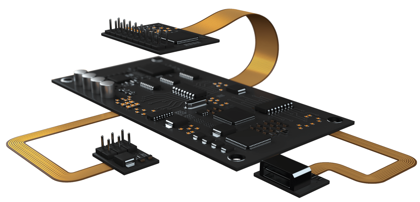
PCB Designing Services
Develop custom PCB designs tailored to product requirements, performance goals, circuit functionality, and hardware integration needs.

PCB Layout Services
Create optimized PCB layouts with efficient routing, component placement, signal management, and production-ready board structures.

PCB Development Services
Support end-to-end PCB development including design refinement, prototyping, testing coordination, and production preparation.

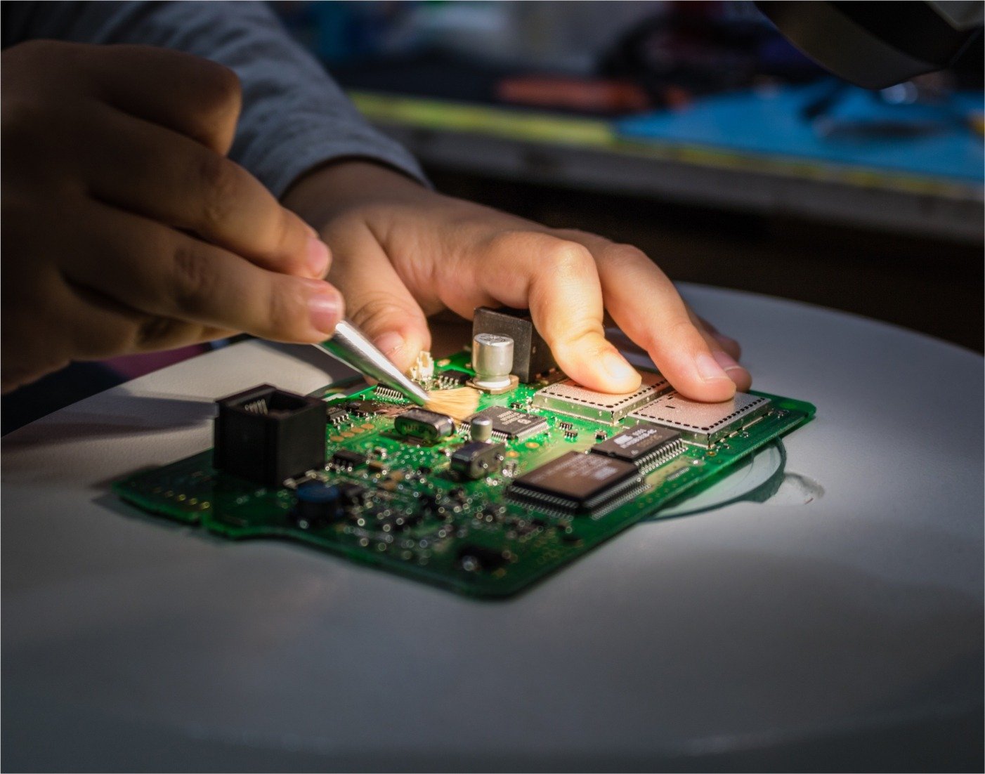
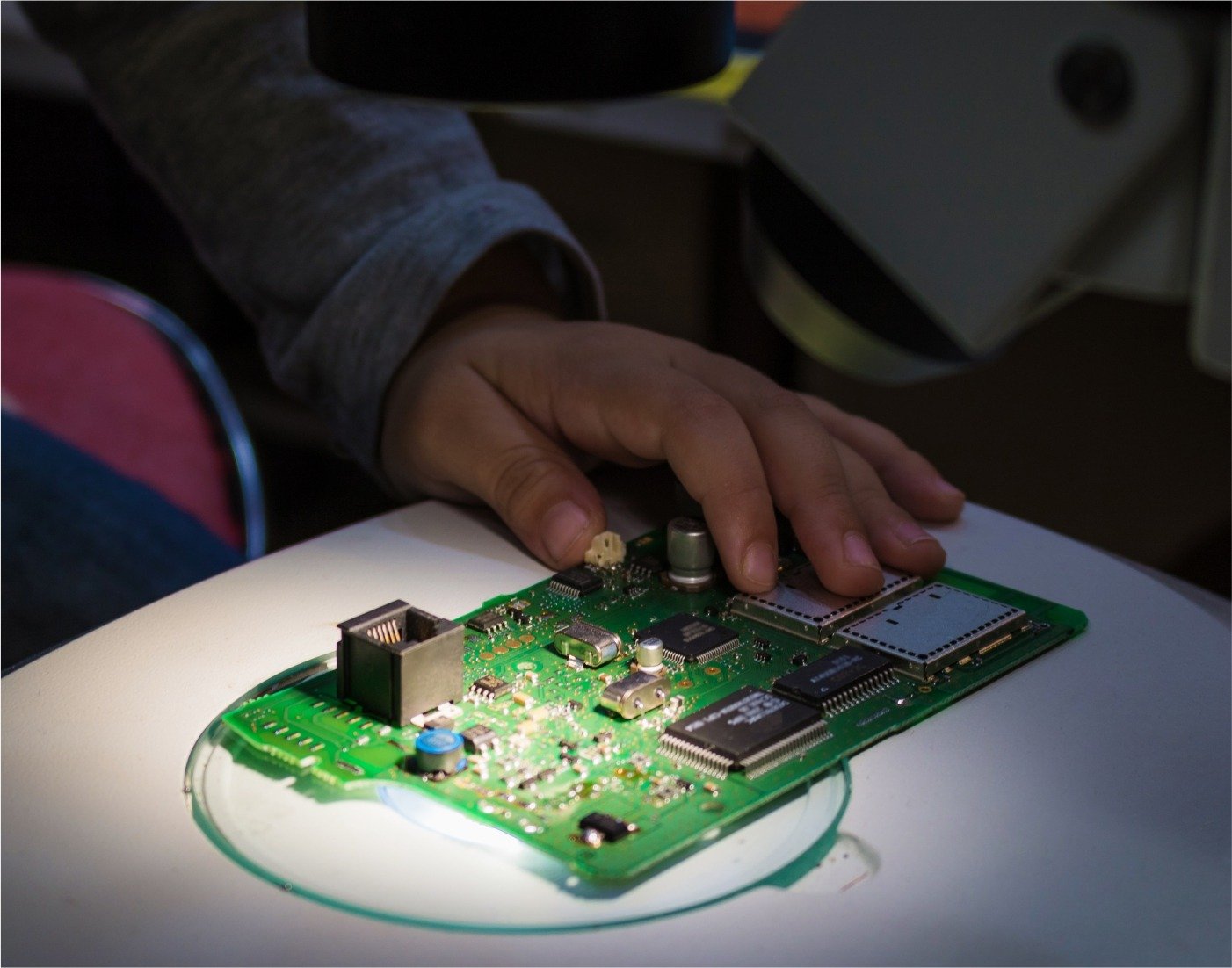
PCB Verification & Testing
Perform design verification, electrical validation, functional testing, and quality checks to improve board reliability and stability.

Documentation Services
Prepare manufacturing files, BOMs, Gerber files, assembly documentation, design specifications, and technical records accurately.

Memory Layout Solutions
Design efficient memory layouts for embedded systems, high-speed boards, and performance-critical hardware applications.

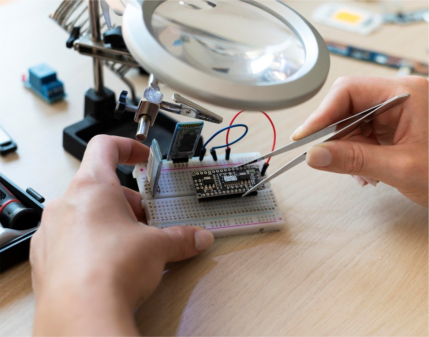
PCB Prototyping Services
Develop PCB prototypes for functional validation, testing workflows, design optimization, and production readiness evaluation.

High-Density Designs
Create compact, multilayer, and high-density PCB designs optimized for advanced electronic products and complex hardware systems.
With Tools That Strengthen Layout and Validation
Prepare Your PCB for Real-World Testing


Not Just Schematics or Components
Why Reliable Electronics Depend on PCB Design Quality
- Signal Integrity
- EMI Control
- Thermal Stability
- Manufacturability
Optimize routing and electrical performance to reduce signal loss, interference, timing issues, and communication instability.
Implement shielding strategies, grounding techniques, and layout optimization to minimize electromagnetic interference.
Design thermal management systems that improve heat dissipation, board reliability, and long-term hardware performance.
Ensure PCB designs align with fabrication standards, assembly requirements, testing workflows, and scalable manufacturing processes.
With Our 5-Step PCB Designing Process
Move from Concept to Production Without Failure
Create detailed circuit schematics, component selection plans, and hardware architecture aligned with product specifications.
Develop optimized PCB layouts with routing precision, signal integrity management, and efficient component placement.
Prepare production-ready manufacturing files and coordinate PCB fabrication processes for quality-controlled output.
Support PCB assembly workflows, component integration, soldering coordination, and assembly validation processes.
Perform functional testing, verification checks, electrical analysis, and final validation before deployment or production scaling.
PCB Designing Questions
Let Our Specialists Answer Your
Remote PCB designers can manage schematic creation, layout design, routing, prototyping support, testing coordination, manufacturing documentation, and design optimization workflows.
Yes, production-ready PCB design involves manufacturability checks, signal integrity analysis, thermal management, testing validation, and fabrication alignment processes.
Project complexity determines resource requirements. Some PCB designers can manage end-to-end workflows, while advanced systems may require collaboration across hardware, firmware, and testing specialists.
PCB designers coordinate through Gerber files, BOM documentation, fabrication specifications, assembly requirements, testing standards, and production communication workflows.
Common causes include poor routing, thermal issues, EMI interference, incorrect component placement, inadequate testing, and manufacturability inconsistencies.
Design security is maintained through secure communication systems, controlled file access, confidentiality agreements, protected repositories, and structured operational workflows.